Home
Ohio Tech Companies: Fast-Track Your R&D
Partner with Nanotech West Lab's expert team to transform your innovations into market-ready solutions. Through the Ohio Sensor and Semiconductor Innovation Platform (OSSIP), our experienced scientists and engineers will help optimize your processes and develop breakthrough products.
Ready to advance your technology?
Contact Jay DeLombard through email or by calling 614-292-0774.
OSSIP's Innovation Impact in Ohio
From solo entrepreneurs to established mid-sized companies, OSSIP has partnered with diverse Ohio businesses to launch new product lines. Our track record includes helping five companies transform their concepts into market-ready solutions.

Protect Your Intellectual Property
Your intellectual property is protected. While no proprietary information disclosure is required, we offer complimentary Confidential Disclosure Agreements to companies who wish to share sensitive details.
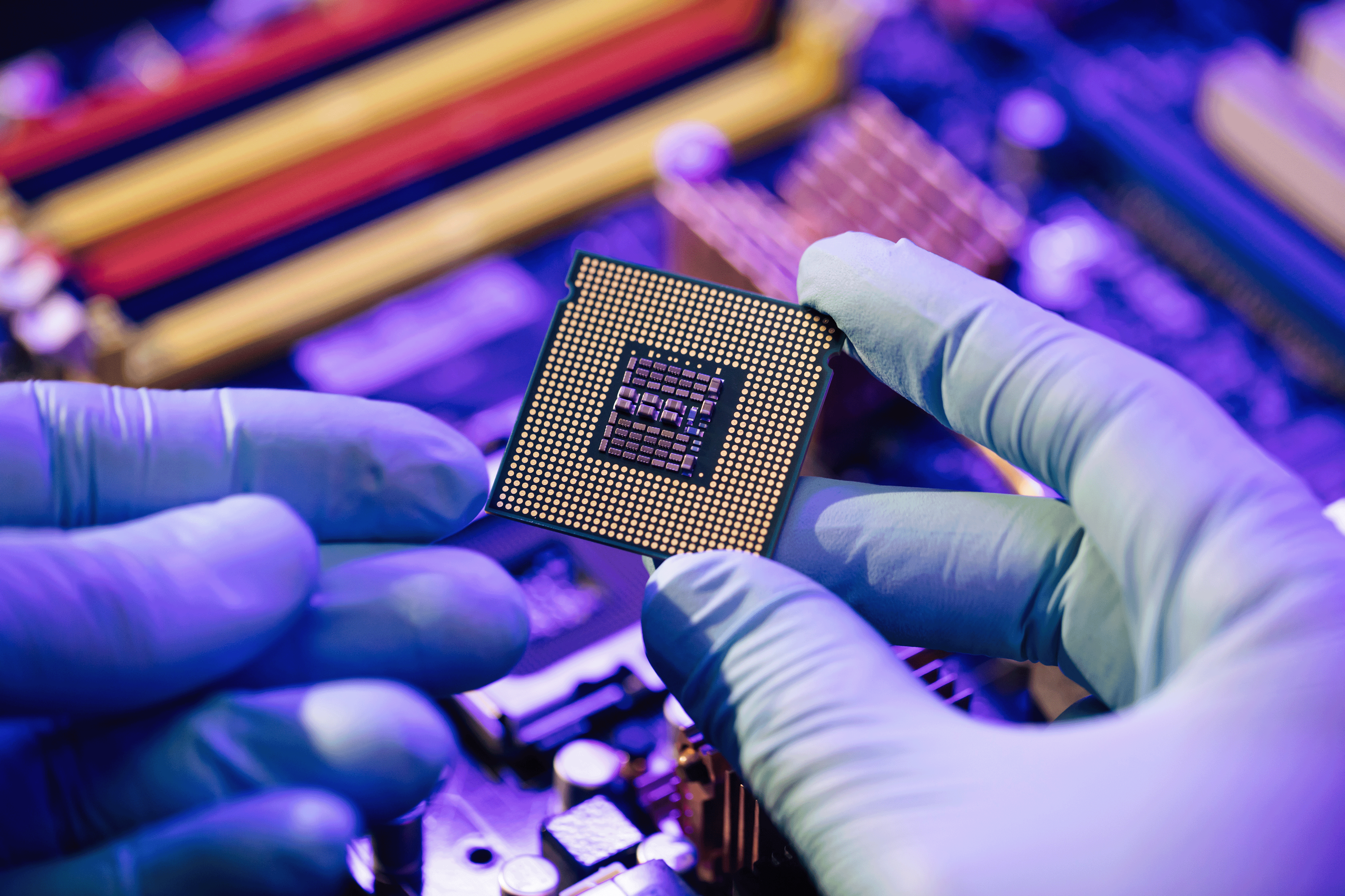
Accelerate Your Innovation with World-Class Capabilities
From sub-20nm electron beam lithography to III-V compound semiconductor growth, our comprehensive facilities span the complete spectrum of modern microfabrication. Access state-of-the-art equipment including MOCVD, atomic layer deposition, and precision analytical tools—all supported by expert guidance to accelerate your development process.
1 Metalorganic Chemical Vapor Deposition Epitaxial Growth
Aixtron metalorganic chemical vapor deposition (MOCVD) of III-V materials capable of growing (In, Al, Ga) (As, P, Sb) compound semiconductors
2 Scanning Electron Microscopy
Imaging, composition and spectroscopy for failure mode investigation and structure analysis
3 Lapping and Chemical-Mechanical Polishing
Logitech PM4 lapping using alumina, norbide, diamond; Logitech PM5 polishing using Nalco CMP suspensions
4 Picosun SUNALE Atomic Layer Deposition
Lower temperature oxides and nitrides of zinc, aluminum, hafnium, titanium, tantalum
5 Electron Beam Lithography
Lithography down to sub-20nm or better, photomask layout and fabrication
6 E-Beam Evaporation Coating
Electron-beam evaporation of Ag, Al, Au, Cr, Ge, Ni, Pd, Pt, Ti, Mo, and more
7 Sputter Deposition
Metallic and reactive sputtering of Ag, Al, Al2O3 , Co, Cr, Cu, Fe, ITO, Mo, Nb, Nb2O5, Ni, NiCr (80/20%), NiFe, SiO2, Ti, V, W, W/Ti (10/90%)
1 Photolithography
Spin coating of photoresists; contact and step-and-repeat exposure systems; Heidelberg µPG 501 maskless direct-write lithography tool; two standard spin-on glass processes
2 K&S 7100 Precision Dicing Saw
Dicing of all different substrate materials, including silicon, sapphire, glass quartz, fused silica, SiC, GaN, InP, LiNbO3, LiTaO3
3 Reactive Ion Etching
High precision inductively-coupled plasma reactive ion etching of most materials using BCl3, CF4, O2, CHF3, Cl2, Ar
4 Chemical Processing
Four cleanroom wet benches available for cleaning and etching processes
5 Chemical Vapor Deposition Of Silicon Oxides And Nitrides
PECVD of silicon oxide and silicon nitride using simple preprogrammed routines in the Plasmatherm 790; LPCVD stoichiometric or low-stress silicon nitride processes
6 Microscopy and Measurement
High precision microscopy and photography of samples, as well as atomic force microscopy with biological imaging capability, ellipsometry and nanometrics thin-film measurement systems
7 Thermal Processing
Rapid thermal annealers, tube furnaces, and ovens are all available for any custom processing required, carbon nanotube deposition